Wednesday, December 5, 2007

TYPES OF ANTENNAS

TYPES OF ANTENNAS

Introduction

This report discusses the common types of antennas available, their design and their attributes, which includes the radiation patterns, the gain and bandwidth characteristics.

Antenna Types

There are basically three classifications of antennas: Dipole, Reflector and Yagi. But the aggregate difference is in the design, as will be discussed.

The Dipole

This is the simplest TV antenna. Variations on the dipole are the bowtie, the folded-dipole and the loop (a difference on the folded dipole). All four have the same gain and the same radiation field: a torroid (doughnut shape). The gain is generally 2.15 dB.The dipole has positive gain because it does not radiate equally in all directions. To get more gain, an antenna must radiate in fewer directions. If one rotates an antenna about the forward axis (a line from the transmitting antenna) the signal strength will vary as the cosine of the angle. In other words, when the antenna elements are vertical, no signal is received because TV signals have horizontal polarization

Stacked Dipoles

N number of dipoles will take in N times as much RF power as one dipole, provided they are not too close to each other. Thus a 4-dipole antenna would have a gain of 8.15 dB. Dipoles are commonly stacked horizontally (collinearly), vertically (broadside), and in echelon (end-fire).

When dipoles are stacked horizontally, the horizontal beam width becomes very narrow. This is because they do not add in-phase for directions not straight ahead. Similarly, when stacked vertically, the vertical beam width becomes narrower. A lot of dipoles stacked vertically would give the gain you needed. The vertical narrowness of the resulting beam is of little importance, but the horizontal broadness of the beam means no rotor needed.
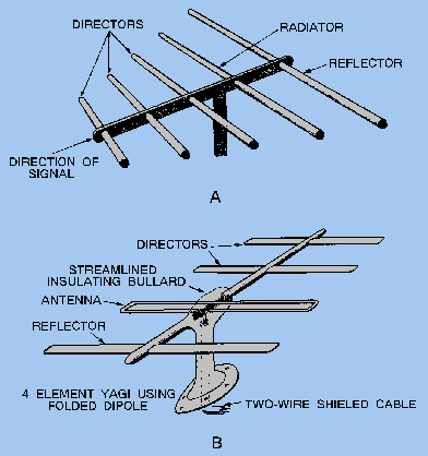


Yagi Antennas

A Yagi antenna has several elements arranged in echelon. They are connected together by a long element, called the boom. The boom carries no current. If the boom is an insulator, the antenna works the same.

The rear-most element is called the reflector. The next element is called the driven element. All the remaining elements are called directors. The directors are about 5% shorter than the driven element. The reflector is about 5% longer than the driven element. The driven element is usually a folded dipole or a loop. It is the only element connected to the cable, yet the other elements carry almost as much current. The more directors added, the higher the gain becomes. Gains above 20 dB are possible. But the Yagi is a narrowband antenna, often intended for a single frequency. As frequency increases above the design frequency, the gain declines abruptly. Below the design frequency, the gain falls off more gradually. When a Yagi is to cover a band of frequencies, it must be designed for the highest frequency of the band. An antenna has an aperture area, from which it captures all incoming radiation. The aperture of a Yagi is round and its area is proportional to the gain. As the leading elements absorb power, diffraction bends the adjacent rays in toward the antenna.


Reflector Antennas

Radio waves will reflect off of a large conducting plane as if it was a mirror. A coarse screen will serve as well. Reflector antennas are very common.

The double bow-tie screen reflector shown above has an average gain of 6 dB. With a bigger screen it would have more. The parabolic reflector focuses the signal onto a single dipole, but its bandwidth is a little disappointing. The corner reflector has a little less gain but much greater bandwidth. The corner reflector has roughly the gain of three dipoles. It is a good medium gain antenna, widely used for UHF.

Log-Periodic Dipole Arrays (LPDA)

The LPDA has several dipoles arranged in echelon and criss-cross fed from the front. The name comes from the geometric growth, which is logarithmic.


Reference:

  • Common Antenna Types, a HDTV primer © http://www.hdtvprimer.com/ANTENNAS


Tuesday, December 4, 2007

Assignment 7: RF filter designs


FILTER DESIGNS IN RF


Filters in electronics are divided into two broad categories

  • Passive filters
  • Active filters


In this assignment we are going to be consider mainly the passive filters
The passive filters are also divided into five categories

  • Low pass filter

  • High pass filter

  • Band pass filter

  • Band stop filter

  • Notch filter


High-pass filter
A high-pass filter is a filter that passes high frequencies well, but attenuates (or reduces) frequencies lower than the cutoff frequency. The actual amount of attenuation for each frequency varies from filter to filter. It is sometimes called a low-cut filter; the terms bass-cut filter or rumble filter are also used in audio applications. A high-pass filter is the opposite of a low-pass filter, and a band pass filter is a combination of a high-pass and a low-pass.
It is useful as a filter to block any unwanted low frequency components of a complex signal while passing the higher frequencies. Of course, the meanings of 'low' and 'high' frequencies are relative to the cutoff frequency chosen by the filter designer.


Band-stop filter

A generic ideal band-stop filter, showing both positive and negative angular frequencies
In signal processing, a band-stop filter or band-rejection filter is a filter that passes most frequencies unaltered, but attenuates those in a specific range to very low levels. It is the opposite of a band-pass filter. A notch filter is a band-stop filter with a narrow stop band (high Q factor). Notch filters are used in live sound reproduction (Public Address systems, also known as PA systems) and in instrument amplifier (especially amplifiers or preamplifiers for acoustic instruments such as acoustic guitar, mandolin, bass instrument amplifier, etc.) to reduce or prevent feedback, while having little noticeable effect on the rest of the frequency spectrum. Other names include 'band limit filter', 'T-notch filter', 'band-elimination filter', and 'band-rejection filter'.

Band-pass filter

A band-pass filter is a device that passes frequencies within a certain range and rejects (attenuates) frequencies outside that range. An example of an analogue electronic band-pass filter is an RLC circuit (a resistor-inductor-capacitor circuit). These filters can also be created by combining a low-pass filter with a high-pass filter.
An ideal filter would have a completely flat pass band (e.g. with no gain/attenuation throughout) and would completely attenuate all frequencies outside the pass band. Additionally, the transition out of the pass band would be instantaneous in frequency. In practice, no band pass filter is ideal. The filter does not attenuate all frequencies outside the desired frequency range completely; in particular, there is a region just outside the intended pass band where frequencies are attenuated, but not rejected. This is known as the filter roll-off, and it is usually expressed in dB of attenuation per octave or decade of frequency. Generally, the design of a filter seeks to make the roll-off as narrow as possible, thus allowing the filter to perform as close as possible to its intended design. However, as the roll-off is made narrower, the pass band is no longer flat and begins to "ripple." This effect is particularly pronounced at the edge of the pass band in an effect known as the Gibbs phenomenon.


Low pass filters


An ideal low-pass filter completely eliminates all frequencies above the cut-off frequency while passing those below unchanged. The transition region present in practical filters does not exist. An ideal low pass filter can be realized mathematically (theoretically) by multiplying a signal by the rectangular function in the frequency domain or, equivalently, convolution with a sine function in the time domain.


5. All-pass filter

An all-pass filter is an electronic filter that passes all frequencies equally, but changes the phase relationship between various frequencies. It does this by varying its propagation delay with frequency. Generally, the filter is described by the frequency at which the phase shift crosses 90°. They are generally used to compensate for other undesired phase shifts that arise in the system, or for mixing with an unshifted version of the original to implement a notch comb filter. They may also be used to convert a mixed phase filter into a minimum phase filter with an equivalent magnitude response or an unstable filter into a stable filter with an equivalent magnitude response Reference:

Ref

http://www.play-hookey.com/ac_theory/hi_pass_filters.html
http://en.wikipedia.org/wiki/Special:Search?search=high+-pass+filters&go=Go
http://www.altavista.com/web/results?itag=ody&q=types+of+filter+designs&kgs=0&kls

Assignment 5

RF AMPLIFIERS
RF amplifiers are classified A, AB, B or C according to the phase-angle (number of degrees of current flow during each 360-degree RF cycle) over which plate- or collector-current flows.
Class A AmplifiersClass A amplifiers operate over a relatively small portion of a tube’s plate-current or a transistor’s collector-current range and have continuous plate- or collector-current flow throughout each RF cycle. Their efficiency in converting DC-source-power to RF-output-power is poor. DC source power that is not converted to radio frequency output power is dissipated as heat. However, in compensation, Class A amplifiers have greater input-to-output waveform linearity (lower output-signal distortion) than any other amplifier class. They are most commonly used in small-signal applications where linearity is more important than power efficiency, but also are sometimes used in large-signal applications where the need for extraordinarily high linearity outweighs cost and heat disadvantages associated with poor power efficiency.
Class B AmplifiersClass B amplifiers have their tube control-grids or transistor bases biased near plate- or collector-current cutoff, causing plate- or collector-current to flow only during approximately 180 degrees of each RF cycle. That causes the DC-source-power to RF-output-power efficiency to be much higher than with Class A amplifiers, but at the cost of severe output cycle waveform distortion. That waveform distortion is greatly reduced in practical designs by using relatively high-Q resonant output “tank” circuits to reconstruct full RF cycles.
The effect is the same in principle as pushing a child in a swing through half-swing-cycles and letting the natural oscillatory characteristics of the swing move the child through the other half-cycles. However, low sine-wave distortion results in either case only if the Q of the oscillatory circuit (the tank circuit or the swing) is sufficiently high. Unless the Q is infinite, which it never can be, the amplitude of one-half cycle will be larger than the other, which is another way of saying there always will be some amount of harmonic energy. (Coupling an antenna system too tightly to the resonant output tank circuit of an amplifier will lower its Q, increasing the percentage of harmonic content in the output.)
Another effective method commonly used to greatly reduce Class B RF amplifier output waveform distortion (harmonic content) is to employ two amplifiers operating in “push-pull” such that one conducts on half-cycles where the other is in plate- or collector-current cutoff. Oscillatory tank circuits are still used in the outputs of Class B push-pull amplifiers to smooth switching transitions from the conduction of one amplifier to the other, and to correct other nonlinearities, but lower-Q tank circuits can be used for given percentages of harmonic content in the output. (Tank circuits can be loaded more-heavily for given percentages of harmonic output where two amplifiers operate in push-pull.)
Class AB AmplifiersAs the designation suggests, Class AB amplifiers are compromises between Class A and Class B operation. They are biased so plate- or collector-current flows less than 360 degrees, but more than 180 degrees, of each RF cycle. Any bias-point between those limits can be used, which provides a continuous selection-range extending from low-distortion, low-efficiency on one end to higher-distortion, higher-efficiency on the other.
Class AB amplifiers are widely used in SSB linear amplifier applications where low-distortion and high power-efficiency tend to both be very important. Push-pull Class AB amplifiers are especially attractive in SSB linear amplifier applications, because the greater linearity resulting from having one amplifier or the other always conducting makes it possible to bias push-pull Class AB amplifiers closer to the Class B end of the AB scale where the power-efficiency is higher. Alternatively, push-pull Class AB amplifiers can be biased far enough toward the highly-linear Class A end of the scale to make broadband operation without resonant tank circuits possible in applications where broadband operation or freedom from tuning is more important than power-efficiency.
Class C AmplifiersClass C amplifiers are biased well beyond cutoff, so that plate- or collector-current flows less than 180 degrees of each RF cycle. That provides even higher power-efficiency than Class B operation, but with the penalty of even higher input-to-output nonlinearity, making use of relatively high-Q resonant output tank circuits to restore complete RF sine-wave cycles essential. High amplifying-nonlinearity makes them unsuitable to amplify AM, DSB, or SSB signals.
However, most Class C amplifiers can be amplitude-modulated with acceptably low distortion by varying plate- or collector-voltage, because they generally are operated in the region of plate- or collector-saturation so that the RF output voltage is very closely dependent upon instantaneous DC plate- or collector-voltage. They also are commonly used in CW and frequency-shift-keyed radiotelegraph applications and in phase- and frequency-modulated transmitter applications where signal amplitudes remain constant.


Reference

Assignment 6

cellular phone block diagram of RF section


The RFphone mainly is to regulate and modulate the high radio frequency. This is done when the cell phone is active, that is the phone is either reciving a signal or sending one.

without the RF section of the phone the will not be able to communicate with the one another.

The RF section also in a phone amplifies the recived IF signal and mixes it with the carrier frequency from the local oscillator ( LO )


Assignment 4

ASSIGNMENT4


MICROWWAVE SYSTEMS

Electromagnetic (EM) radiation is a self-propagating wave in space with electric and magnetic components. These components oscillate at right angles to each other and to the direction of propagation, and are in phase with each other. Electromagnetic radiation is classified into types according to the frequency of the wave: these types include, in order of increasing frequency, radio waves, microwaves, terahertz radiation, infrared radiation, visible light, ultraviolet radiation, X-rays and gamma rays.

Microwaves are electromagnetic waves with wavelengths shorter than one meter and longer than one millimeter, or frequencies between 300 megahertz and 300 gigahertz. The microwave range includes ultra-high frequency (UHF) (0.3–3 GHz), super high frequency (SHF) (3–30 GHz), and extremely high frequency (EHF) (30–300 GHz) signals. A microwave oven works by passing microwave radiation, usually at a frequency of 2450 MHz (a wavelength of 12.24 cm), through the food. Water, fat, and sugar molecules in the food absorb energy from the microwave beam in a process called dielectric heating. Many molecules (such as those of water) are electric dipoles, meaning that they have a positive charge at one end and a negative charge at the other, and therefore rotate as they try to align themselves with the alternating electric field induced by the microwave beam. This molecular movement creates heat as the rotating molecules hit other molecules and put them into motion.

Microwave radio is used in broadcasting and telecommunication transmissions because, due to their short wavelength, highly directive antennas are smaller and therefore more practical than they would be at longer wavelengths (lower frequencies). There is also more bandwidth in the microwave spectrum than in the rest of the radio spectrum; the usable bandwidth below 300 MHz is less than 300 MHz while many GHz can be used above 300 MHz. Typically, microwaves are used in television news to transmit a signal from a remote location to a television station from a specially equipped van.

Microwave frequency bands

The microwave spectrum is usually defined as electromagnetic energy ranging from approximately 1 GHz to 1000 GHz in frequency, but older usage includes lower frequencies. Most common applications are within the 1 to 40 GHz range. Microwave Frequency Bands as defined by the Radio Society of Great Britain in the table below:

Designation Frequency range

L band 1 to 2 GHz

S band 2 to 4 GHz

C band 4 to 8 GHz

X band 8 to 12 GHz

Ku band 12 to 18 GHz

K band 18 to 26.5 GHz

Ka band 26.5 to 40 GHz

Q band 30 to 50 GHz

U band 40 to 60 GHz

V band 50 to 75 GHz

E band 60 to 90 GHz

W band 75 to 110 GHz

F band 90 to 140 GHz

D band 110 to 170 GHz


Reference

  • http://books.google.co.uk/books?id=1eCEcxtMhucC&pg=PA489&ots=Sd9-hAllXt&dq=%27block+diagram+microwave+system
  • http://wiki.answers.com/Q/What_were_people%27s_first_reactions_to_the_microwave_when_it_first_came_out

Assignment 3

ASSIGNMENT 3

LIST OF SPECIAL COMPONENTS USED IN RF SYSTEMS

There are very many active components that are used in RF systems. the main ones we will list in this assignments are the active components with will include transistors, diode, inductive circuits and switches. The respective clusters are PIN Diodes, Varactor Diodes, and Band Switch Diodes.

DIODE BAND SWITCHES

Digit-Key Part Number

Manufacturer Part Number

Description

BA277 T/R-ND

BA277 T/R

DIODE BAND-SWITCHING SOD523

BA591 T/R-ND

BA591 T/R

DIODE BAND-SWITCHING SOD323

BA792 T/R-ND

568-1912-2-ND

BA792 T/R

DIODE BAND-SWITCHING SOD110

BA891 T/R

DIODE SWITCH BAND 35V SOD-523

568-1913-2-ND

BAP1321-02 T/R

DIODE PIN 60V 100MA SOD-523

568-1914-2-ND

BAP1321-03 T/R

DIODE PIN 60V 100MA SOD-323

BAP1321-04 T/R-ND

BAP1321-04 T/R

DIODE PIN 60V 100MA SOT-23

568-1915-2-ND

BAP50-02 T/R

DIODE PIN 50V 50MA SOD-523

568-1922-2-ND

BAP51-03 T/R

DIODE PIN GP 50V 50MA SOD-323

568-1923-2-ND

BAP51-05W T/R

DIODE PIN GP 50V 50MA SOT-323

568-1924-2-ND

BAP51L T/R

DIODE PIN 60V 100MA SOD-882

568-1925-2-ND

BAP55L T/R

DIODE PIN 50V 100MA SOD-882

568-1938-2-ND

BAP65-03 T/R

DIODE PIN 30V 100MA SOD-323

568-1939-2-ND

BAP65-05W T/R

DIODE PIN 30V 100MA SOT-323

568-1940-2-ND

BAP70-02 T/R

DIODE PIN 50V 100MA SOD-523

568-1941-2-ND

BAP70-03 T/R

DIODE PIN 50V 100MA SOD-323

568-1942-2-ND

BAP70-05 T/R

DIODE PIN 50V 100MA SOT-23

568-1944-2-ND

BB131 T/R

DIODE VHF VAR CAP 30V SOD323

BB135 /T3-ND

BB135 /T3

DIODE UHF VAR CAP 30V SOD323

BB135 T/R-ND

BB135 T/R

DIODE UHF VAR CAP 30V SOD323

568-3425-2-ND

BB141 T/R

DIODE VAR CAP 6V SOD-523

568-3426-2-ND

BB143 T/R

DIODE VAR CAP 6V SOD-523

568-3427-2-ND

BB145 T/R

DIODE VAR CAP 6V SOD-523

BB184 T/R-ND

BB184 T/R

DIODE UHF VAR CAP 13V SOD523

568-1950-2-ND

BB187 T/R

DIODE VHF VAR CAP 32V SOD523

568-1954-2-ND

BB207 T/R

DIODE FM VAR CAP 15V SOT-23

BB208-02 /T3-ND

BB208-02 /T3

DIODE VAR CAP 10V 20MA SOD523

BB208-02 T/R-ND

BB208-02 T/R

DIODE VAR CAP 10V 20MA SOD523

BB208-03 /T3-ND

BB208-03 /T3

DIODE VAR CAP 10V 20MA SOD323

BGY66B-ND

BGY66B

IC AMPLIFIER REVERSE SOT115J

BGY67-ND

BGY67

IC AMPLIFIER REVERSE SOT115J

BGY67A-ND

BGY67A

IC AMPLIFIER REVERSE SOT115J

BGY68-ND

BGY68

IC AMPLIFIER REVERSE SOT115J

BGY685A-ND

BGY685A

IC PUSH-PULL AMP 600MHZ SOT115J

BGY687-ND

BGY687

IC PUSH-PULL AMP 600MHZ SOT115J

BGY888-ND

BGY888

IC PUSH-PULL AMP 860MHZ SOT115J

BLA0912-250-ND

BLA0912-250

TRANS LDMOS NCH 75V SOT502A

BLA1011-10-ND

BLA1011-10

TRANS LDMOS NCH 75V SOT467C

BLA1011S-200-ND

BLA1011S-200

TRANS LDMOS NCH 75V SOT502B

568-2388-ND

BLF245B

TRANSISTOR RF DMOS SOT279A

568-2403-ND

BLF246B

TRANSISTOR RF DMOS SOT161A

568-2389-ND

BLF248

TRANSISTOR RF DMOS SOT262A1

568-2412-ND

BLF278

TRANSISTOR RF DMOS SOT262A1

BLS2731-50 TRAY-ND

BLS2731-50 TRAY

TRANSISTOR RF POWER SOT422A

568-4080-ND

OM7600/BGA2001/1800

EVAL BOARD FOR BGA2001

568-4081-ND

OM7600/BGA2001/900

EVAL BOARD FOR BGA2001

568-4082-ND

OM7619/BGA2003

EVAL BOARD FOR BGA2003


Tuesday, October 30, 2007

ASSIGNMENT 2

IMPORTANCE OF SMITH CHARTS IN RF SYSTEMS

What's a Smith chart?

What is a Smith chart? It's really just a plot of complex reflection overlaid with an impedance and/or admittance grid referenced to 1-ohm characteristic impedance. That's it! Transmission coefficient, which equals unity plus reflection coefficient, may also be plotted (see below). You can find books and articles describing how a Smith chart is a graphical representation of the transmission line equations and the mathematical reasons for the circles and arcs, but these things don't really matter when you need to get the job done. What matters knows the basics and how to use them, like always.

The Smith chart contains almost all possible impedances, real or imaginary, within one circle. All imaginary impedances from - infinity to + infinity are represented, but only positive real impedances appear on the "classic" Smith chart. Yes, it is possible to go outside the Smith chart "unity" circle, but only with an active device because this implies negative resistance.

One thing you give up when plotting reflection coefficients on a Smith chart is a direct reading of a frequency axis. Typically, plots that are done over any frequency band have markers calling out specific frequencies.

Why use a Smith chart?

Use of the Smith Chart utility has grown steadily over the years and it is still widely used today, not only as a problem solving aid, but as a graphical demonstrator of how many RF parameters behave at one or more frequencies, an alternative to using tabular information. The Smith Chart can be used to represent many parameters including impedances, admittances, reflection coefficients, a Smith chart is the RF engineer's best friend! It's easy to master, and it adds an air of "analog coolness" to presentations, which will impress your friends, if not your dates! A master in the art of Smith-charting can look at a thoroughly messed up VSWR of a component or network, and synthesize two or three simple networks that will impedance-match the circuit in his head!

Reference:

  1. Chris Bowick.RF Circuits design. 1982, Oxford, Boston.
  2. www.wikipedia.org/smithcharts